결정 성장
★ crystal growth [반도체] 결정 성장.
The silicon substrate for microelectronic chips must be made of a single crystal whose unit cell is oriented in a certain direction. The properties of the substrate and the way it is processed are both infl uenced by these requirements. Accordingly, silicon used as the raw material in semiconductor device fabrication must not only be of ultra high purity, as in electronic grade silicon; it must also be prepared in the form of a single crystal and then cut in a direction that achieves the desired planar orientation. The crystal-growing process is covered here, and the next section details the cutting operation.
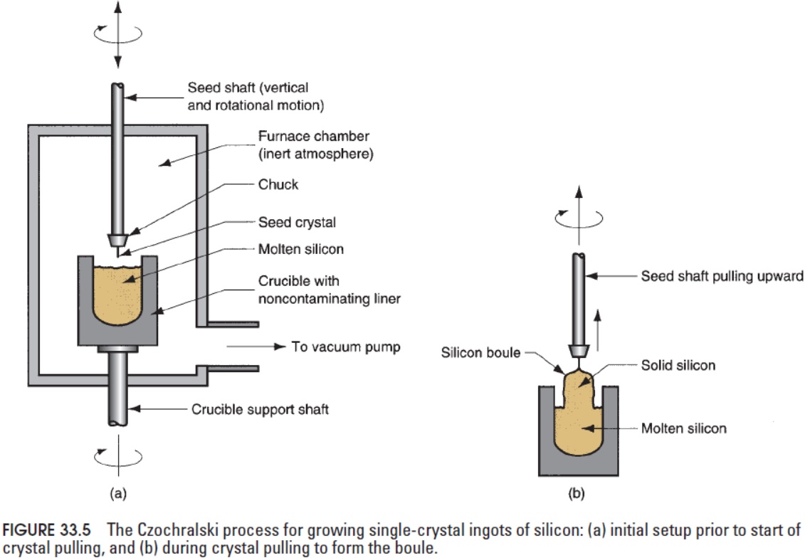
The most widely used crystal-growing method in the semiconductor industry is the Czochralski process, illustrated in Figure 33.5, in which a single crystal ingot, called a boule, is pulled upward from a pool of molten silicon. The setup includes a furnace, a mechanical apparatus for pulling the boule, a vacuum system, and support ing controls. The furnace consists of a crucible and heating system contained in a vacuum chamber. The crucible is supported by a mechanism that permits rotation during the crystal-pulling procedure. Chunks of EGS are placed in the crucible and heated to a temperature slightly above the melting point of silicon: 1410°C (2570°F). Heating is by induction or resistance, the latter being used for large melt sizes. The molten silicon is doped5 before pulling begins to make the crystal either p-type or n-type.
To initiate crystal growing, a seed crystal of silicon is dipped into the molten pool and then withdrawn upward under carefully controlled conditions. At fi rst the pulling rate (vertical velocity of the pulling apparatus) is relatively rapid, which causes a single crystal of silicon to solidify against the seed, forming a thin neck. The velocity is then reduced, causing the neck to grow into the desired larger diameter of the boule while maintaining its single crystal structure. In addition to pulling rate, rotation of the crucible and other process parameters are used to control boule size. Single-crystal ingots of diameter = 450 mm (18 in) and up to 3 m (10 ft) long can be produced for subsequent fabrication of microelectronic chips.
The most widely used crystal-growing method in the semiconductor industry is the Czochralski process, illustrated in Figure 33.5, in which a single crystal ingot, called a boule, is pulled upward from a pool of molten silicon. The setup includes a furnace, a mechanical apparatus for pulling the boule, a vacuum system, and support ing controls. The furnace consists of a crucible and heating system contained in a vacuum chamber. The crucible is supported by a mechanism that permits rotation during the crystal-pulling procedure. Chunks of EGS are placed in the crucible and heated to a temperature slightly above the melting point of silicon: 1410°C (2570°F). Heating is by induction or resistance, the latter being used for large melt sizes. The molten silicon is doped5 before pulling begins to make the crystal either p-type or n-type.
To initiate crystal growing, a seed crystal of silicon is dipped into the molten pool and then withdrawn upward under carefully controlled conditions. At fi rst the pulling rate (vertical velocity of the pulling apparatus) is relatively rapid, which causes a single crystal of silicon to solidify against the seed, forming a thin neck. The velocity is then reduced, causing the neck to grow into the desired larger diameter of the boule while maintaining its single crystal structure. In addition to pulling rate, rotation of the crucible and other process parameters are used to control boule size. Single-crystal ingots of diameter = 450 mm (18 in) and up to 3 m (10 ft) long can be produced for subsequent fabrication of microelectronic chips.
[출처: Mikell P. Groover, Fundamentals of Modern Manufacturing Materials, Processes, and Systems]