광리소그래피
★ optical lithography
Optical lithography uses light radiation to expose a coating of photoresist on the surface of the silicon wafer; a mask containing the required geometric pattern for each layer separates the light source from the wafer, so that only the portions of the photoresist not blocked by the mask are exposed. The mask consists of a fl at plate of transparent glass onto which a thin fi lm of an opaque substance has been deposited in certain areas to form the desired pattern. Thickness of the glass plate is around 2 mm (0.080 in), whereas the deposited fi lm is only a few mm thick—for some film materials, less than one mm. The mask itself is fabricated by lithography, the pattern being based on circuit design data, usually in the form of digital output from the CAD system used by the circuit designer.
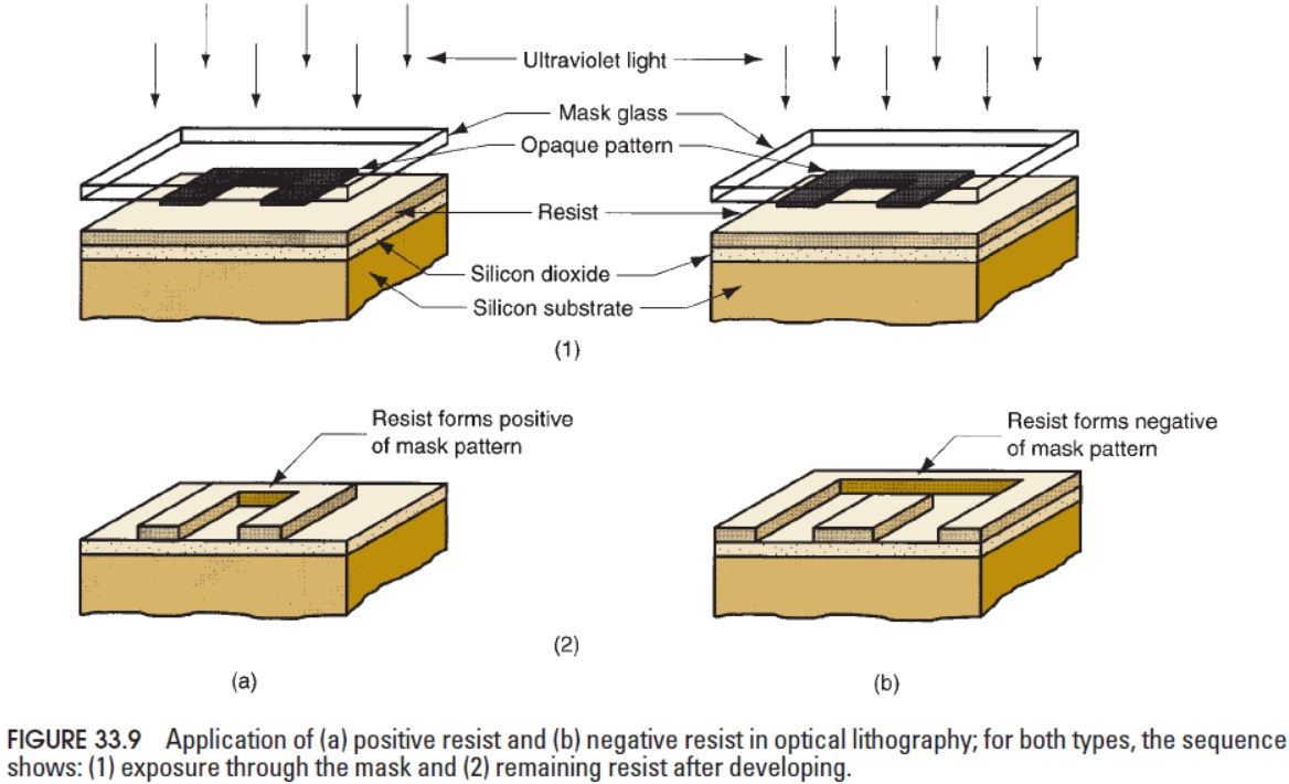
[출처: Mikell P. Groover, Fundamentals of Modern Manufacturing Materials, Processes, and Systems]
★ photolithography